Z80NG — Z80 Next Gen
The Z80NG is a Z80N-compatible CPU soft core designed for the eZX Spectrum and related Spectrum-lineage FPGA platforms. It implements the full Z80N instruction set as used by the ZX Spectrum Next, including all Next-specific opcode extensions, while adding microarchitectural enhancements (instruction prefetch buffer, μop cache, unlocked turbo mode) that take effective performance far beyond what any silicon Z80 ever delivered.
The Z80NG is a clean-room reimplementation of the Z80N ISA — original logic design, not derived from any existing Z80N source. See License and origin.
The same chip design is intended for reuse across multiple FPGA images:
- ZX Spectrum Next compatibility — DDR3-backed system RAM, 28 MHz cycle-accurate or unlocked turbo
- Classic Spectrum and compatibles — BSRAM-backed system RAM, 3.5 / 7 MHz cycle-accurate per model (Z80N extensions disabled to match the original Z80)
- Third-party Spectrum-lineage FPGA projects — licensable under the open-source terms documented below
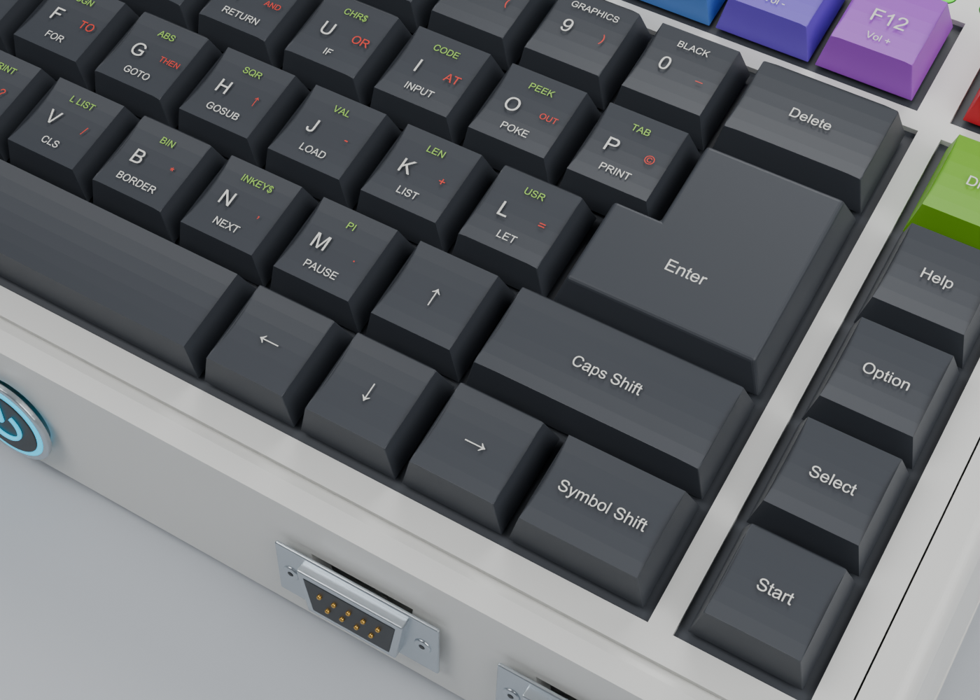
Concept render — white keyboard cursor cluster and right Caps Shift up close.
ISA compatibility
Z80 base instruction set
Full Z80 ISA: all 8-bit and 16-bit arithmetic, logic, shift / rotate, bit manipulation, block transfer, I/O, branch, call / return, and prefix opcodes (CB, DD, ED, FD, DDCB, FDCB). The complete Z80 flag model (S, Z, Y, H, X, P/V, N, C) is implemented with the documented and undocumented behaviours that real Z80 software depends on. The IR pair, IM 0 / 1 / 2 interrupt modes, refresh cycle accounting, and the standard NMI behaviour are all in place.
Undocumented opcodes (the IX / IY half-register set, SLL, LD r,(IX+d) variants, etc.) behave identically to the original Zilog Z80. This is essential for compatibility with real-world software and demos that depend on these instructions.
Z80N extensions
When operating in Z80N mode, the Z80NG also implements the Spectrum Next's extended instruction set:
PUSH nn(push immediate)OUTINB(output increment B)LDIRSCALE(scaled block copy)LDIX,LDDX,LDIRX,LDDRX,LDPIRX(extended block transfers)LDWS(line-stride block copy for sprites and tiles)BSLA,BSRA,BSRL,BSRF,BRLC(barrel shifts)MIRROR(bit-reverse A)MUL D,E(8 × 8 → 16 hardware multiply)ADD HL,A/ADD DE,A/ADD BC,A(8-bit add to 16-bit pair)ADD HL,nn/ADD DE,nn/ADD BC,nn(16-bit immediate add)SWAPNIB(swap nibbles of A)TEST nn(test immediate against A)NEXTREG(Next register access — paired with the chipset NEXTREG infrastructure)
Z80N opcode timings match the Spectrum Next reference at the cycle-accurate 28 MHz mode.
Mode selection
The Z80NG has two ISA modes selected per power-on reset (or by chipset register at image initialisation):
| Mode | Z80N extensions | Refresh accounting | Use case |
|---|---|---|---|
| Z80 strict | Disabled — execute as illegal-instruction / NOP per the original Z80 | Standard Z80 R-register refresh | Classic Spectrum image (16K, 48K, 128K, +2, +2A, +3, Pentagon, Timex, Didaktik, Scorpion) |
| Z80N | Enabled — all Spectrum Next extensions active | Standard Z80 R-register refresh | Next-compatible image |
The mode is a single bit; the rest of the CPU is identical. This means the Z80NG is one design serving both the Classic Spectrum image and the Next-compat image, configured at instantiation time.
Microarchitecture
Pipeline overview
The Z80NG is a multi-stage pipeline with stages tuned for variable-length Z80 instruction handling:
- Prefetch — pulls bytes from memory into the prefetch buffer
- Length / decode — determines instruction length (1–4 bytes for Z80, up to 4 for Z80N extensions) and decodes to μop format
- μop cache check — looks up the instruction in the μop cache; on hit, bypasses decode
- Operand fetch — reads source registers and any immediate data from the μop
- Execute — ALU, shift, memory address generation
- Memory — load / store, with rendezvous to the nominal Z80 clock in cycle-accurate mode
- Writeback — register file update, flag update
The pipeline length is implementation-dependent and may vary between cycle-accurate and turbo modes. In cycle-accurate mode the visible CPU behaviour is timing-locked to the nominal Z80 M-cycle / T-state structure; the pipeline depth is hidden behind that lock. In turbo mode the pipeline runs at full FPGA clock with no rendezvous, exposing the deep pipeline directly.
Instruction prefetch buffer
A windowed byte buffer occupying one full BSRAM block (18 Kbit, ~2 KB usable for buffer data plus tag/control bits) holds memory bytes around the current PC, with PC positioned in the middle of the window rather than at one end. The window slides forward as the PC advances: the forward edge is filled in advance from DDR3 in 64-byte BL8 bursts, and the trailing portion behind the current PC is retained as long as it remains within the window's address range. The BSRAM block is dual-ported so the background prefetcher writes the forward edge on one port while the fetch stage reads on the other — no contention.
This windowed design is critical for Z80 performance because of the language's loop idiom. Z80 software relies heavily on tight backward branches — DJNZ (decrement B, jump if non-zero), JR NZ,addr, LDIR/LDDR/CPIR/OUTI block ops with implicit backward iteration. A typical Z80 inner loop is 4–30 bytes; a typical Z80 function body is 50–500 bytes. With PC in the middle of a ~2 KB window (~1 KB ahead + ~1 KB behind):
| Branch type | Distance from PC | Cost |
|---|---|---|
| Forward branch within window | up to +1 KB | Free — advance the read pointer |
| Backward branch within window | up to −1 KB | Free — rewind the read pointer |
| Forward branch outside window | > +1 KB | Refetch from new PC |
| Backward branch outside window | < −1 KB | Refetch from new PC |
Function-scale working set capture. A function up to ~1 KB fits entirely in the backward half of the window once entered; every backward branch within it (loops, retries, error paths, dispatch returns) is free of memory cost. Multiple consecutive small functions called in sequence can share the buffer — when one function calls another and the callee fits in the forward half, no refetch is needed at the call boundary either. The buffer is sized to capture the working set of a typical Z80 hot path, not just one inner loop.
When refetch happens. Refetch costs one DDR3 round-trip (~50 ns) and a refill burst. With ~2 KB of window, refetch is rare in realistic Z80 code: cold function entry from cold callers, long jumps (JP nnnn across pages), interrupt entry, returns from deep call chains, table-driven dispatch where the target is far from current PC. The amortised cost across realistic execution is small — most cycles spend execution time inside the buffer's address range.
Forward branches into the window — common for short conditional skips (JR Z,addr+5 and similar) — are similarly free, just like the backward case. The Z80's typical "skip a few bytes" pattern doesn't trigger any DDR3 traffic.
The window itself is keyed by address, not by position-relative-to-PC. A taken branch that lands anywhere within the window's current address range is free; the read pointer simply moves to the new position within the same valid byte range. This is conceptually a small single-set fully-associative byte cache for the active code region, but implemented as a simple sliding window with no tag array — just a base address and length, much cheaper in LUTs than a real cache while delivering most of the benefit for code with reasonable locality.
Combined with the μop cache — which holds decoded μops for the hot ~4 KB of Z80 code, see μop cache — the prefetch buffer's job is to keep the cold-miss path fast and absorb DDR3 latency from cold μop fills. Hot code runs from the μop cache; warm code runs from prefetch buffer + μop cache cold-miss; cold code pays a DDR3 round-trip + decode latency once on first execution. In turbo mode this layered design delivers single-cycle dispatch at the full 380 MHz BSRAM clock for the dominant hot-path case.
μop cache
The Z80's variable-length instruction encoding (1–4 bytes, with up to two prefix bytes and various addressing modes) is the principal obstacle to high FPGA clock rates. The μop cache solves this by translating each decoded Z80 instruction into a fixed 4-byte μop and caching the result in BSRAM. The execute path then becomes a fixed-width read-and-execute machine — vastly simpler timing, much higher achievable fmax.
μop format
| Field | Bits | Purpose |
|---|---|---|
| Internal op code | 8 | ~256 internal operations (ALU, M-cycle templates, special ops) |
| Source operand | 4 | Register A–L, (HL), (IX+d), (IY+d), immediate, etc. |
| Destination operand | 4 | Register A–L, (HL), (IX+d), (IY+d) |
| Immediate / displacement | 8 | Low byte of nn or signed d |
| Flag affect mask | 4 | Which Z80 flags this op writes |
| M-cycle count | 4 | For cycle-accurate timing in cycle-accurate mode |
| Total | 32 bits | One 4-byte μop |
Some Z80 instructions decode to multiple μops (block ops, prefixed indirections, conditional behaviour). The decoder emits the μop sequence into the cache as a small linked list keyed by the original Z80 PC and paging state.
Cache configuration
| μop cache size | Z80 code coverage | BSRAM cost | Typical hit rate |
|---|---|---|---|
| 4 KB | 1024 μops (~2 KB of Z80 code) | 2 BSRAM blocks | 70–85% on tight loops |
| 8 KB | 2048 μops (~4 KB of Z80 code) | 4 BSRAM blocks | 85–95% on game inner loops |
| 16 KB (default) | 4096 μops (~8 KB of Z80 code) | 8 BSRAM blocks | 95%+ on demo and game workloads |
| 32 KB | 8192 μops (~16 KB of Z80 code) | 16 BSRAM blocks | 98%+ for entire 48K Spectrum hot paths |
The default is 16 KB, which uses about 3% of the GW5AST-LV138 BSRAM budget — comfortably fits alongside line buffers, sprite tables, and the prefetch buffer. Tag arrays add about 1 KB more for the index-to-Z80-PC mapping with paging state.
Self-modifying code handling
Some Spectrum and Next software (tape loaders, demo intros, decompression routines, protection schemes) writes to memory addresses then executes them. The μop cache maintains a dirty-page bit vector — 256 bits for 64 KB of address space, paged per Spectrum bank. A Z80 store to a page with cached μops invalidates those μops; subsequent execution re-decodes from the new bytes.
Paging and bank changes
The Spectrum 128 / +2 / +3 paging registers ($7FFD, $1FFD) and the Z80N's extended paging registers all change which RAM bank is mapped into the Z80's address space. Cached μops are keyed by the simulated Z80 address at decode time — so when paging changes, the μops that were correct for the previous mapping are no longer correct for the new mapping at the same Z80 addresses.
Handling this without per-bank tag overhead: the μop cache is flushed on any paging-register write. This is the cleanest mechanism for two reasons:
- Paging writes are rare — typically once per scene transition, level load, or major mode change. The cache rebuild after a flush completes within the first few thousand instructions of the new code path, after which performance returns to fully-cached
- The alternative (tagging each μop with its bank-state at decode) would require ~8 additional bits per μop and a per-cycle comparison against the current paging state, adding both BSRAM cost and timing-closure pressure
The flush is also applied on Z80NG ISA mode change (Z80 strict ↔ Z80N ↔ Z80NG-extended), on IM mode change, and on interrupt entry to a different code region if the trace pattern shows that's beneficial. These are all infrequent events; the μop cache hit rate stays at 95%+ in steady-state execution.
For pathological SMC-heavy code (rare) the worst case is that the μop cache provides no acceleration — performance degrades to prefetch-buffer-only speed (a lower effective clock, set by decode combinational depth at ~200–250 MHz) rather than full turbo at the BSRAM-limited 380 MHz. The CPU never misbehaves; the only penalty is missed speedup.
Multi-cycle operations and stall-on-use scoreboard
Many Z80NG operations take more than one internal cycle to complete:
MUL D,E(Z80N hardware multiply, 8 × 8 → 16): 1–2 internal cycles in the FPGA DSP block- FPGA-native extensions (
BLKCPYblock copy, wide arithmeticADD HLDE,BCDE, parallel byte ops): 1 to many cycles depending on operation - DDR3 memory reads on the Next-compatible image: up to ~19 cycles for a first-byte cache miss
- DDR3 writes: variable stall when the Write FIFO can't accept more
- Future Z80NG-extended divisions (if added): tens of cycles
Without architectural help, every multi-cycle operation would stall the pipeline for its full latency before the next instruction could issue. The Z80NG avoids this with a destination-register scoreboard — a standard Tomasulo-style mechanism that lets operations complete out of order while preserving the architecturally-observable single-issue order:
- Each architectural register (A, B, C, D, E, H, L, the shadow set A'/B'/C'/D'/E'/H'/L', IX, IY, SP, F, F', I, R, IFF1, IFF2, IM) has a single "valid" bit, initially set to true
- When an instruction issues, the destination register's valid bit is cleared
- The instruction enters its operation-specific pipeline (multiplier, ALU, memory unit, block engine) and runs to completion in parallel with subsequent instructions
- Subsequent instructions can dispatch immediately if their source registers are all valid (the in-flight op's destination is not one of their sources)
- An instruction whose source register has a cleared valid bit stalls until the in-flight op completes and sets the valid bit
- When the multi-cycle operation finishes, it writes its result to the destination register and sets the valid bit
The mechanism is cheap — about 25 valid bits (one per architectural register) plus comparison logic at instruction issue. Roughly 100 LUT4s for the entire scoreboard, with the comparison fitting comfortably in the FPGA fabric without adding to the critical path.
Example: MUL D,E followed by independent code:
MUL D,E      ; D,E pending — multiplier starts; D,E valid bits cleared
LD A,(HL)    ; reads HL (valid), writes A — issues immediately, runs in parallel
ADD A,B      ; reads A,B (both valid), writes A,F — issues immediately
LD C,A       ; reads A (valid), writes C — issues immediately
             ; ... by now the multiplier has completed; D,E are valid again
LD H,D       ; reads D (now valid) — no stall
Four instructions following the MUL all dispatch without stalling. The multiplier runs in parallel with them. Only a code path that immediately reads D or E after the MUL would stall — and even then, only until the multiplier completes (1–2 cycles).
Example: stall-on-use:
MUL D,E      ; D,E pending
LD A,D       ; reads D — STALL until multiplier finishes
             ; pipeline resumes
The stall is minimal — just the multiplier's remaining latency — and recovers immediately. The same single-instruction stall would be the entire MUL execution time on a real Z80N.
Multi-register destinations:
Some operations write multiple architectural registers. The scoreboard clears all of them on issue:
| Instruction | Cleared destination registers |
|---|---|
MUL D,E |
D, E (16-bit result) |
ADD HL,DE (16-bit add) |
H, L, F |
LD HL,(nn) (16-bit load) |
H, L |
LDIR (block copy, per iteration) |
B, C, H, L, D, E, F |
EX DE,HL (register swap) |
Single cycle — D, E, H, L stay valid throughout |
BLKCPY (Z80NG-extended) |
H, L, D, E, B, C, F |
POP BC (16-bit pop) |
B, C |
Memory operations:
Loads (LD A,(HL), LD A,(nn), LD A,(IX+d)) also use the scoreboard. The destination register is marked pending; the load issues to the memory controller; subsequent independent instructions dispatch; the load completes whenever the data arrives (DDR3 round-trip, BSRAM single-cycle, or prefetch-buffer hit) and the destination is marked valid. Read-after-write hazards are caught by the standard scoreboard logic; pending stores in the Write FIFO are snooped automatically (see Write path).
Interaction with cycle-accurate mode:
In cycle-accurate modes (3.5 / 7 / 14 / 28 MHz), the scoreboard runs internally but is invisible externally — the rendezvous mechanism still ties software-visible memory accesses to the per-T-state boundary, so multi-cycle operations like MUL D,E still appear to take their full 8 T-states from the software's perspective. The scoreboard just lets the internal logic pre-execute and avoid actual FPGA-cycle stalls, freeing the multiplier and other functional units to start work early. No software-visible timing changes in cycle-accurate mode — purely a microarchitectural acceleration.
In turbo mode (no rendezvous), the scoreboard is the primary mechanism for hiding multi-cycle latency. Most realistic Z80 code has enough instruction-level parallelism between multi-cycle ops and their use that pipeline stalls are rare.
In cycle-accurate mode (3.5 MHz, 7 MHz, 14 MHz, or 28 MHz), the Z80NG's internal pipeline runs at the full FPGA clock — far faster than the nominal Z80 clock — and uses memory operations as rendezvous points to stay in sync with what a real Z80 at the nominal clock would have done. The mechanism is:
- The pipeline runs ahead, executing μops at the BSRAM-limited FPGA clock
- Each μop carries the official Z80 T-state count that its source instruction would have consumed on real silicon (this is the M-cycle count field in the μop encoding)
- As μops retire, an accumulator tracks the total Z80 T-states the program would have consumed so far
- Just before any memory operation (load, store, opcode fetch, port I/O) the pipeline stalls and waits until elapsed real time × nominal Z80 clock ≥ accumulated Z80 T-states
- Once the inequality is satisfied, the memory operation proceeds; the pipeline resumes running ahead
The result is that software-visible memory accesses happen at exactly the same wall-clock time as on a real Z80 at the nominal clock — to within one FPGA clock period — even though the internal logic has been running faster between rendezvous points. ULA contention, floating bus, raster-precise timing tricks, tape-loader edge timing, and copper-coordinated graphics all see the same per-cycle behaviour as on real hardware.
This is the same accumulator used by the Z80-equivalent T-state counter — the cycle-accurate rendezvous and the empirical effective-frequency measurement share the same underlying mechanism.
Operating modes
Spectrum cycle-accurate mode
| Model | Nominal Z80 clock | Source compatibility |
|---|---|---|
| ZX Spectrum 16K / 48K / + | 3.5 MHz | Bit-exact original timing including ULA contention and floating bus |
| ZX Spectrum 128 / +2 / +2A / +3 | 3.5 MHz | As above; +3 floppy timing handled at chipset level |
| Pentagon 128 | 3.5 MHz (no contention) | Russian-clone-compatible |
| Timex TS2068 / TC2048 | 3.58 / 3.5 MHz | Timex high-resolution modes supported at chipset level |
| Scorpion ZS-256 / Turbo+ | 3.5 / 7 MHz | Turbo+ 7 MHz mode supported |
In this mode the Z80NG uses BSRAM-backed system memory (from the host image's BSRAM allocation) rather than DDR3. BSRAM is single-cycle deterministic, matching the original SRAM in the Spectrum exactly. The μop cache is optional in this mode — performance is already capped by the nominal Z80 clock, so the cache provides only a power and timing-slack benefit, not a speed benefit.
Next compatibility mode (28 MHz)
The Next's standard 28 MHz Z80N mode. Cycle-accurate to the Spectrum Next reference. DDR3-backed system memory via the prefetch buffer; data reads and writes rendezvous with the 28 MHz nominal Z80 clock to preserve software-observable timing. The μop cache is active but its speedup is masked by the 28 MHz lock; in this mode the cache mainly contributes timing-closure slack on the FPGA fabric, not effective MIPS.
Turbo / unlocked mode
The architectural showcase. With no rendezvous to a nominal Z80 clock, the Z80NG runs at the full FPGA core clock — the same 380 MHz clock the eZX primary image uses, which is set by the GW5AST-LV138's BSRAM fmax (the Z80NG's μop cache, prefetch buffer, and pipeline state live in BSRAM, so the core clock can't exceed BSRAM speed). The μop cache delivers its full ~1.7–2× boost over the prefetch-only design by removing the variable-length Z80 decode logic from the critical path.
Existing software that depends on cycle-accurate Z80 timing (which is most pre-modern Spectrum software) does not work correctly in turbo mode — turbo is for software written or recompiled specifically for the eZX. New Z80 software targeting "eZX Z80 turbo" gets a CPU capable of:
- Real-time 3D wireframe and filled-polygon rendering with software clipping
- Multi-voice tracker engines and software FM synthesis at modern bitrates
- Real-time zlib-class compression / decompression while streaming
- Game AI with behaviour trees and live pathfinding
- Interpreted languages (FORTH, BASIC variants, small Lua-style runtimes) at usable speeds
- Even small JIT compilers running in the Z80's native address space
Mode is selectable at image boot via the chipset / AntOS launcher; software opts in.
Speed control register
The Z80NG reuses the Spectrum Next's NextReg $07 (the CPU Speed register) as its mode-select interface, extending the existing 2-bit speed field by one bit to allow the Z80NG-only turbo mode. The bit comes from previously-reserved space, so existing Z80N software writes (which leave the reserved bits at zero) continue to select the same speed they always did:
NextReg $07 write format on Z80NG:
| Bits | Field | Notes |
|---|---|---|
[7:3] |
Reserved | Must be written as 0 |
[2:0] |
Programmed CPU speed | Extended from the Z80N's 2-bit field by claiming bit 2 |
Speed field values:
| Value | Mode | Source |
|---|---|---|
%000 |
3.5 MHz cycle-accurate | Z80N-compatible (matches Z80N %00) |
%001 |
7 MHz cycle-accurate | Z80N-compatible (matches Z80N %01) |
%010 |
14 MHz cycle-accurate | Z80N-compatible (matches Z80N %10) |
%011 |
28 MHz cycle-accurate | Z80N-compatible (matches Z80N %11); includes Next wait state behaviour — see Data-side timing below |
%100 |
56 MHz | Z80NG-only intermediate speed |
%101 |
112 MHz | Z80NG-only intermediate speed |
%110 |
224 MHz | Z80NG-only intermediate speed |
%111 |
Unlocked turbo (~380 MHz, BSRAM-limited) | Z80NG-only — runs at the full FPGA core clock, capped by BSRAM fmax |
NextReg $07 read format on Z80NG:
| Bits | Field | Notes |
|---|---|---|
[7:6] |
Reserved | Read as 0 |
[5:3] |
Current actual CPU speed | Reflects what the CPU is actually running at (may differ from programmed when restricted by other policy — e.g., Layer 2 auto-slowdown, expansion bus enable, debug halt) |
[2:0] |
Programmed CPU speed | What was last written to [2:0] |
The current-speed field is also widened to 3 bits (was bits 5:4 on Z80N, now bits 5:3 on Z80NG). When the Z80NG reports speed %111 in the current-speed field, the CPU is actively running at unlocked turbo. When the programmed speed is %111 but current speed reports a lower value, some policy is restricting the actual clock (most commonly: a debug halt has paused execution, or the Classic image is running in a per-model fixed cycle-accurate mode that overrides programmable speed).
Compatibility implications:
- Existing Z80N software writes 2-bit values (
%00–%11); the high reserved bit remains zero; the Z80NG behaves identically to a Z80N including cycle-accurate timing and all chipset behaviours (sprite drops at line edges, etc.) - Z80NG-aware software writes
%100–%111to access the higher speeds. Writing any bit-2-set value (any speed%1xx) is the unified opt-in to all eZX-extended behaviours — not just the higher CPU clock but also the contention-free sprite engine, full-instruction debug trace, and other chipset enhancements that don't preserve cycle-accurate Next behaviour. The reasoning is architectural: cycle accuracy is already broken by running at a non-28-MHz clock, so once that line is crossed, the chipset can engage its enhanced modes too - This means
$07bit 2 is the single eZX-extension surface — no separate registers for sprite-engine opt-in or other chipset features. Z80N software that never sets bit 2 sees real-Next behaviour; eZX-targeted software that sets bit 2 gets the full eZX-extended chipset - The Classic Spectrum image ignores writes to
$07— its CPU speed is set by the host image's model selection, not by software-programmable register access. Reads still report the current speed; writes are silently dropped. This preserves Spectrum binary compatibility for any software that pokes$07thinking it's running on a Next (the original Spectrum range had no such register, so any access is a Next-aware-software anomaly anyway)
Data-side timing
The Z80NG's windowed prefetch buffer handles instruction fetch latency completely — sequential code and tight loops see no DDR3 delay. Data reads and writes are a separate matter, because their target addresses are computed by the program and aren't predictable far enough in advance to fully hide DDR3 latency at higher CPU clocks.
The Z80NG's strategy depends on the selected mode:
At cycle-accurate Next compatibility (28 MHz), the Z80NG matches the real Spectrum Next's wait state behaviour exactly. The Next adds +1 wait state per M1 opcode fetch and +1 wait state per memory read or write at 28 MHz, because the Next's memory subsystem can't sustain a clean 28 MHz transaction rate. This makes:
| Instruction | T-states at 3.5 MHz | T-states at 28 MHz | Reason |
|---|---|---|---|
NOP |
4 | 5 | +1 M1 fetch wait |
LD A,(HL) |
7 | 9 | +1 M1, +1 memory read |
LD A,(nn) |
13 | 14 | +1 M1, +1 memory read (3 reads needed for full instruction) |
LD (HL),A |
7 | 9 | +1 M1, +1 memory write |
LDIR (per iter) |
21 | 23 | +1 M1, +1 read, +1 write |
The effective Next speed at "28 MHz" is therefore ~21–24 MHz in real-world terms — and the Z80NG replicates this exactly. Software depending on these timings (synchronised demos, raster effects, precise audio, copper-co-ordinated graphics) works identically to a real Spectrum Next. The Z80NG's DDR3 + prefetch + run-ahead is technically capable of running a "true" 28 MHz with no wait states, but the cycle-accurate mode deliberately throttles to match the Next.
At 3.5 / 7 / 14 MHz cycle-accurate modes, no wait states are needed — DDR3 access (~50 ns) is comfortably within the T-state budget at these speeds (143–285 ns per T-state). The Z80NG matches the real Next behaviour, which also adds no wait states at these speeds.
At Z80NG-only speeds (56 / 112 / 224 MHz), there is no Spectrum Next behaviour to match. The Z80NG defines its own timing:
| Mode | T-state period | DDR3 access (~50 ns) | Behaviour |
|---|---|---|---|
| 56 MHz | 18 ns | ≈ 2.8 T-states | Run-ahead absorbs most cost; +1–2 wait states on cold data reads |
| 112 MHz | 8.9 ns | ≈ 5.6 T-states | Run-ahead absorbs sequential cost; +4–5 wait states on cold data reads |
| 224 MHz | 4.5 ns | ≈ 11 T-states | Memory-access-dominant; effective speed depends heavily on locality |
At these higher speeds, the Z80NG's effective performance depends on how data access patterns interact with the DDR3 latency budget. Sequential data streams (LDIR / LDDR block copies, sequential reads through HL) benefit from the run-ahead memory issue mechanism — the address is known early enough for DDR3 to deliver in time. Random pointer indirection (LD A,(HL) immediately after HL was computed) may stall.
At unlocked turbo (%111), there are no timing guarantees. Memory accesses pay their natural DDR3 latency. The CPU runs as fast as the FPGA logic allows on instruction execution and stalls naturally on uncached data fetches. This mode is for software written specifically for the Z80NG; cycle-accurate timing is explicitly out of scope.
In the Classic Spectrum image (BSRAM-backed memory), all of this is moot. BSRAM is single-cycle deterministic at the FPGA clock. At any Z80NG speed up to unlocked turbo, BSRAM delivers data well within the T-state budget — no wait states are needed at any mode in the Classic image. This is one of the architectural wins of putting Classic system RAM in BSRAM: the cycle-accuracy story is inherently clean across all CPU speeds because the memory subsystem is fast enough that the question never arises.
Run-ahead and speculative addressing. For data reads, the Z80NG's decode stage attempts to issue the DDR3 access as soon as the source address is known. For Z80 instructions where the address comes from a register (LD A,(HL), LD A,(IX+d)), the address is available at decode time if the register isn't being modified by an earlier in-flight instruction. For instructions where the address comes from immediate operands (LD A,(nn)), the address is fully known at decode and the DDR3 access starts immediately. This run-ahead is what makes the higher Z80NG-only speeds (56 / 112 / 224 MHz) usable in practice — typical Z80 code has enough address-known-early patterns that most data accesses can be overlapped with the preceding instructions.
Write path
Memory writes cannot truly complete in one Z80NG cycle when the target is DDR3. A single DDR3 write transaction takes ~50 ns end-to-end (address, command, data setup), which at the 380 MHz core clock is ~19 cycles — the same kind of latency as a read, in the opposite direction. The Z80NG handles this with a write FIFO between the CPU's writeback stage and the DDR3 controller.
How the write FIFO works:
- Each retired write (Z80 store, push, block-op byte) pushes one entry into the FIFO: address + data + width (8 / 16 / 64 bits)
- The FIFO drains to DDR3 in the background, opportunistically coalescing sequential writes into BL8 bursts where possible
- From the CPU pipeline's perspective, a write retires in one cycle (the FIFO push) regardless of how long the actual DDR3 transaction takes
- The CPU stalls only when the FIFO is full — sustained write rates higher than DDR3 can absorb
The FIFO is sized to comfortably handle realistic Z80 write rates. At 380 MHz with one 8-bit Z80 write per cycle worst-case = 380 MB/s; DDR3 sustained write bandwidth is 4–5 GB/s, so DDR3 absorbs writes ~12× faster than the CPU can issue them. A FIFO of 16–32 entries is more than enough headroom; FIFO-full stalls are essentially a non-event in typical Z80 workloads (which write at perhaps 1 byte per 5–10 instructions, not one per cycle).
Read-after-write to a pending address. The FIFO is snoopable from the read path — if a data read targets an address that's currently sitting in the FIFO (a write that hasn't yet committed to DDR3), the read returns the FIFO entry's value rather than the stale DDR3 value. This handles the read-after-write hazard transparently without requiring CPU pipeline stalls.
Cache coherence with the prefetch buffer and μop cache. Writes to addresses inside the prefetch buffer's current window invalidate the affected bytes in the buffer (range check on the write address against the buffer's base + length). Writes to addresses with cached μops set the dirty bit for that page in the μop cache's dirty-page bit vector. Both mechanisms are simple address comparisons triggered at write retire time; no full cache coherence protocol is needed.
The cycle count assumption. All Z80NG cycle figures in this document — 1 cycle for LD (HL),A, 1–2 cycles for LD (nn),HL, 1–2 cycles for PUSH BC, 1 cycle for PUSH nn — assume the write FIFO has room. They represent CPU pipeline retirement cost, not actual DDR3 commit latency. The DDR3 commit happens in the background, ~19 cycles after the FIFO push, but the CPU sees no stall unless the FIFO fills.
In the Classic Spectrum image (BSRAM-backed memory), writes are genuinely single-cycle deterministic — BSRAM completes writes in 1 cycle at the FPGA clock. No FIFO is needed; no buffering, no background commit, no coherence checks. This is another structural advantage of the BSRAM-backed Classic image: the write path is as clean as the read path, and the cycle counts in the tables are exact and observable in real time, not pipeline-buffered.
Future enhancement (v2): write-coalescing or small writeback cache. If profiling shows that hot-spot writes (e.g., per-frame sprite x/y updates, animation frame counters, status registers) would benefit from coalescing repeated writes to the same address, a small (1–2 KB) writeback cache could be added in front of the FIFO. This would be a v2 enhancement; v1's write FIFO is sufficient for the typical Z80 workload profile.
Performance estimates
FPGA clock targets
The Z80NG's μop cache, prefetch buffer, register-file backing store, and pipeline state all live in BSRAM. The Z80NG's core clock therefore cannot exceed the BSRAM fmax — there is no design trick that gets the CPU running faster than the storage it depends on. On the GW5AST-LV138 the BSRAM is rated to 400+ MHz; with realistic timing-closure margin the design target lands at the same 380 MHz as the eZX primary image's core clock.
| Implementation point | Z80NG core clock | Notes |
|---|---|---|
| Prefetch buffer only, no μop cache | 200–250 MHz | Limited by variable-length Z80 decode timing in the combinational decode path |
| Prefetch buffer + 16 KB μop cache (default) | ~380 MHz | Default eZX target — matches BSRAM fmax with timing-closure margin |
| Hypothetical wider FPGA with faster BSRAM | Whatever that BSRAM allows | Not applicable to GW5AST-LV138 |
The μop cache is what unlocks the ~380 MHz target. Without it, the variable-length Z80 decode logic has too much combinational depth to close timing at the full BSRAM clock. With it, the decode work is done once per μop and amortised across many dispatches, so the execute path's critical path becomes a fixed-width read-and-dispatch — bounded by BSRAM access, not by decode combinational logic.
The Z80NG's unlocked turbo mode is therefore "as fast as the BSRAM will allow", not "as fast as conceivable Z80 logic". This is a meaningful architectural ceiling: the Z80NG on GW5AST-LV138 hardware will hit ~380 MHz and stay there, regardless of whatever pipeline aggressiveness is added in software-visible terms. The Arora V family shares the same BSRAM speed across part sizes, so smaller parts hit the same ceiling — the win on a larger part is more LUT4 budget and more BSRAM blocks, not a faster individual block. The eZX Spectrum uses the same FPGA as Ant64's FireStorm, so this ceiling is the same on both hosts.
Cycle counts per Z80 instruction
The 380 MHz physical clock does more work per cycle than a Z80 T-state did. The Z80 ISA was designed around 8-bit datapaths in 1976, so many of its instructions were decomposed into multiple internal microcoded steps that took 4–23 T-states on real silicon. The Z80NG on a modern FPGA has wide datapaths, single-cycle 16-bit ALU, parallel register-file access, and a 72-bit DDR3 / single-cycle BSRAM memory subsystem — so most of those multi-T-state Z80 instructions collapse into 1–3 Z80NG cycles when executed from the μop cache.
Internal cycle costs per Z80 instruction class (μop cache hit, unlocked turbo mode):
Cycle-count assumptions. All counts below are CPU pipeline retirement cycles — what the CPU front-end sees. Memory reads on the DDR3-backed Next-compatible image rely on run-ahead and the prefetch buffer to hide latency; memory writes rely on the write FIFO to absorb DDR3 commit latency (~19 cycles in the background). See Write path for the write architecture, and Data-side timing for read behaviour per mode. The Classic Spectrum image runs from BSRAM and the cycle counts apply directly without any latency-hiding assumptions.
| Z80 instruction | Real Z80 T-states | Z80NG cycles |
|---|---|---|
NOP |
4 | 1 |
LD r,r' (register move) |
4 | 1 |
ADD A,B |
4 | 1 |
ADD HL,DE (16-bit add) |
11 | 1 |
LD HL,(nn) (16-bit load) |
16 | 1–2 |
LD (nn),HL (16-bit store) |
16 | 1–2 |
PUSH BC |
11 | 1–2 |
POP BC |
10 | 1–2 |
LDIR (per iteration) |
21 | 2 (hardware-paced block op) |
JR cc,d taken |
12 | 1 |
CALL cc,nn taken |
17 | 2 |
EX DE,HL |
4 | 1 |
DJNZ d taken |
13 | 1 |
Z80N-specific instructions (the Spectrum Next extensions, implemented by the Z80NG as part of Z80N-compatible mode). All Z80N opcodes use the ED prefix, which costs 4 T-states for the prefix fetch on real Z80N silicon before the operation even begins — even when the operation itself is trivially fast (single-bit reorder, parallel AND, barrel shift). The Z80NG eliminates this prefix overhead through the μop cache and executes most Z80N operations in a single cycle using FPGA primitives:
| Z80N instruction | Encoding | Real Z80N T-states | Z80NG cycles | FPGA primitive enabling the speedup |
|---|---|---|---|---|
SWAPNIB (swap nibbles of A) |
ED 23 |
8 | 1 | LUT-level bit reorder |
MIRROR A (bit-reverse A) |
ED 24 |
8 | 1 | Parallel bit reversal in fabric |
TEST nn (AND-test immediate) |
ED 27 nn |
11 | 1 | Parallel AND + flag update; immediate in μop |
BSLA DE,B (barrel shift left arithmetic) |
ED 28 |
8 | 1 | Native FPGA barrel shifter |
BSRA DE,B (barrel shift right arithmetic) |
ED 29 |
8 | 1 | Native FPGA barrel shifter |
BSRL DE,B (barrel shift right logical) |
ED 2A |
8 | 1 | Native FPGA barrel shifter |
BSRF DE,B (barrel shift right fixed-bit) |
ED 2B |
8 | 1 | Native FPGA barrel shifter |
BRLC DE,B (barrel rotate left circular) |
ED 2C |
8 | 1 | Native FPGA barrel shifter |
MUL D,E (8 × 8 → 16) |
ED 30 |
8 | 1 | GW5AST-LV138 DSP block (18 × 18 multiplier, 400+ MHz) |
ADD HL,A / DE,A / BC,A (8-bit add to 16-bit pair) |
ED 31/32/33 |
8 | 1 | 16-bit ALU |
ADD HL,nn / DE,nn / BC,nn (16-bit add immediate) |
ED 34/35/36 nn nn |
16 | 1 | 16-bit ALU + immediate already in μop |
PUSH nn (push 16-bit immediate) |
ED 8A nn nn |
23 | 1–2 | Immediate in μop; SP decrement + 16-bit store |
OUTINB (output B, increment HL) |
ED 90 |
16 | 2 | Mostly I/O port latency |
NEXTREG nn,nn (set Next register to immediate) |
ED 91 nn nn |
20 | 2 | Chipset register write; both operands in μop |
NEXTREG nn,A (set Next register from A) |
ED 92 nn |
17 | 1–2 | Chipset register write |
PIXELDN (advance HL to next pixel row) |
ED 93 |
8 | 1 | Custom logic for Spectrum screen Y+1 transform |
PIXELAD (build pixel address from D,E coords) |
ED 94 |
8 | 1 | Custom logic for screen address calculation |
SETAE (set A = 1 << (E & 7), pixel-X bitmask) |
ED 95 |
8 | 1 | Decode 3 bits + shift |
JP (C) (jump to (PC_high << 8) ∣ C) |
ED 98 |
13 | 1 | Compose address, take branch |
LDIX (LDI, skip-if-A — sprite transparency) |
ED A4 |
16 | 1–2 | Conditional store; address advance |
LDWS (line-stride byte transfer) |
ED A5 |
14 | 1–2 | Stride add; one byte transferred |
LDDX (LDD, skip-if-A) |
ED AC |
16 | 1–2 | Conditional store; address advance |
LDIRX (per iteration of repeated LDIX) |
ED B4 |
21 / 16 | 1–2 per byte | Hardware-paced block op; potentially 8 bytes per cycle for non-skip case using full DDR3 width |
LDPIRX (per iteration, pattern-based) |
ED B7 |
21 / 16 | 1–2 per byte | Hardware-paced block op |
LDDRX (per iteration of repeated LDDX) |
ED BC |
21 / 16 | 1–2 per byte | Hardware-paced block op |
LDIRSCALE (per iteration, scaled block copy) |
(encoding) | per Z80N spec | 1–2 per byte | Scaler unit + hardware-paced block op |
Why this works so well for Z80N. Most Z80N instructions inherit a 4-T-state ED prefix fetch on real silicon, plus 4+ T-states for the operation itself, even for operations that are trivially fast in FPGA fabric. A single-cycle barrel shift, parallel bit reversal, or LUT-driven nibble swap all pay the same 8-T-state minimum on Z80N silicon because the ED prefix and microcoded execute dominate the cost. The Z80NG sidesteps both: the prefix decode happens once when the μop is built, and the operation itself uses FPGA primitives that already exist in the fabric (the GW5AST-LV138 has DSP blocks rated at 400+ MHz that do 18-bit multiplies in a single cycle — vastly more than MUL D,E's 8 × 8 → 16 needs).
The most dramatic cycle reductions are on the longer Z80N instructions. PUSH nn pays 23 T-states on Z80N silicon — prefix fetch (4) + op fetch (4) + immediate low (4) + immediate high (4) + stack pre-decrement (3) + stack write (4 — actually two stores) — but the Z80NG already has the immediate in the μop after first-time decode, so PUSH nn collapses to a single SP decrement plus a 16-bit BSRAM store: 1–2 cycles. ADD HL,nn collapses from 16 T-states to 1 cycle for the same reason.
Why this works. The μop cache is the critical enabler. Without it, every Z80 instruction would pay the variable-length decode latency on each execution, dominating the cycle cost. With it, the decode is done once per unique instruction and then amortised across thousands of dispatches in a tight loop. Each μop dispatch is a fixed-width read-and-execute that the FPGA can do in one BSRAM cycle. The 16-bit ALU, 72-bit DDR3, and wide register-file access then collapse the Z80's original microcode-step-per-T-state model into single-cycle operations.
When this applies:
- Unlocked turbo mode. In cycle-accurate modes (3.5 / 7 / 14 / 28 MHz), the Z80NG deliberately throttles to match original Z80 / Z80N timing; the internal cycle savings are absorbed by the rendezvous to the nominal clock
- μop cache hit. On a cold miss, the full decode latency applies; sustained-loop workloads hit, one-off code does not
- Memory-bound code is limited by DDR3 latency (~50 ns ≈ 19 cycles at 380 MHz) on the Next-compatible image. The Classic Spectrum image has no such limit because system RAM is in single-cycle BSRAM
- Self-modifying code falls back to prefetch-buffer-only execution when the μop cache is invalidated
Z80-equivalent T-state counter
Rather than projecting an "effective Z80-equivalent clock" speculatively, the Z80NG measures it directly via a hardware debug counter. Every μop carries the T-state count its source Z80 instruction would have consumed on real Zilog silicon (this field already exists in the μop encoding for cycle-accurate rendezvous in cycle-accurate modes — see μop format). Routing the same field into an accumulator costs one adder and a 64-bit BSRAM word.
The counter pair:
| Register | Width | Description |
|---|---|---|
Z80_TSTATE_ACC |
64-bit | Cumulative T-states the executed program would have consumed on a real Z80. Each retired instruction adds its Z80 T-state count |
REAL_CYCLE_ACC |
64-bit | Cumulative FPGA core clock cycles elapsed. Free-running at the BSRAM clock (380 MHz on GW5AST-LV138) |
Both counters are readable over the debug subsystem JTAG path and via a memory-mapped chipset register block for software access during normal execution. Both are resettable (independently or as a pair). 64-bit width gives ~30 years of overflow headroom at 380 MHz even if every cycle retires an instruction.
Computing the effective frequency. Given two counter snapshots (t0_tstate, t0_cycle) and (t1_tstate, t1_cycle):
delta_tstates  = t1_tstate - t0_tstate
delta_cycles   = t1_cycle  - t0_cycle
elapsed_sec    = delta_cycles / FPGA_CLOCK_HZ        ; e.g. 380_000_000
effective_z80_freq_hz = delta_tstates / elapsed_sec
This is a real measurement from a real workload, not a projection. Different workloads produce different numbers; tight register-register loops report one figure, memory-bound code reports another, code using FPGA-native extensions reports a higher figure because those ops contribute their "what this would have cost on a Z80" T-state count even though they execute in 1–2 internal cycles.
Behaviour by mode:
| Mode | What the counter reports |
|---|---|
| Cycle-accurate 3.5 / 7 / 14 / 28 MHz | Effective frequency converges to the nominal Z80 clock — the rendezvous to nominal timing forces real cycles to track T-state period |
| Z80NG 56 / 112 / 224 MHz | Effective frequency reflects whatever balance of cycle compression vs. memory stalls the workload exhibits at that speed |
| Unlocked turbo | Effective frequency depends entirely on workload — register-heavy code reports a high number, memory-bound code reports a lower one |
FPGA-native extensions (when added in v2) contribute their "equivalent Z80 work" T-state cost to the accumulator: BLKCPY for 100 bytes credits 100 × 21 = 2100 T-states, ADD HLDE,BCDE credits ~28 T-states (a chained four-step Z80 sequence). This gives a fair measurement of equivalent Z80 work performed even for instructions that no Z80 ever had.
Why this matters. It moves the cycle-compression story from "we claim the Z80NG performs like a Z80 at X frequency" to "the Z80NG reports the effective frequency it actually achieved on your workload". The number is empirical, reproducible, workload-dependent, and verifiable by anyone with a debugger connection. There's no marketing speculation to defend. If a sceptic asks "does it really go that fast?", the answer is "run your code and read the counter".
Beyond cycle compression: FPGA-native instruction extensions
Cycle compression of existing Z80 instructions is one source of performance improvement. A second source comes from adding new instructions that exploit FPGA internals the Z80 ISA was never designed to express. The Z80 was constrained by 1976 silicon: 8-bit datapath, microcoded execution, no parallel function units, no wide memory access. The Z80NG's FPGA fabric has none of those constraints. Instructions that were impossible to express in Z80 hardware become single-cycle operations on the Z80NG.
Candidate Z80NG-extended instructions:
| Category | Example | Z80 equivalent | Z80NG cost |
|---|---|---|---|
| Wide arithmetic | ADD HLDE,BCDE (32-bit add across register pair concatenations) |
4 separate 8-bit ADC ops, ~28 T-states |
1 cycle |
| Parallel byte ops | SIMD4 ADD A,B,C,D (add 4 byte pairs in parallel) |
4 separate 8-bit ADD A,r ops |
1 cycle |
| Wide memory | LD64 (nn),HLDE'BCHL' (store 8 bytes / 64 bits at once using full DDR3 width) |
8 separate LD (nn),r ops, ~104 T-states |
1–2 cycles |
| Hardware-paced block | BLKCPY (DE),(HL),BC (burst-mode block copy at full DDR3 bus width) |
LDIR at 21 T-states per byte |
~1 cycle per 8 bytes |
| Bit-field | POPCNT HL, CLZ HL, BITREV HL (16-bit population count / count leading zeros / bit reverse) |
Many T-states of shift-and-test | 1 cycle |
| Hardware accelerated patterns | CRC16 HL,A, HASH HL,DE |
Many T-states of inner loop | 1 cycle |
| Pixel ops | PIXBLEND A,B,C (alpha-blend three bytes) |
Manual shift-and-add sequence | 1 cycle |
These are illustrative — exact ISA definitions are future work. The architectural point is that the Z80NG can host instructions that no real Z80 could, and these are then a further source of throughput beyond what cycle compression alone delivers. The internal cycle counts speak for themselves; what they translate to in real workloads depends entirely on instruction mix, memory access pattern, and software design, and is best measured rather than projected.
Third ISA mode for the extensions
To preserve Z80N binary compatibility, the FPGA-native extensions need their own ISA mode:
| Mode | Z80 base ISA | Z80N extensions | Z80NG extensions | Use case |
|---|---|---|---|---|
| Z80 strict | Yes | No | No | Classic Spectrum image — original Z80 software |
| Z80N | Yes | Yes | No | Next-compatible image — Spectrum Next software runs identically |
| Z80NG extended | Yes | Yes | Yes | eZX-specific software targeting the Z80NG's full capability |
The mode is selected at image instantiation time and reported in a feature register so software can detect what's available. Existing Z80N software writes its standard NextReg sequences and runs as on a Next; new eZX-targeted software queries the feature register and uses the extensions when available, falling back to Z80N base when not. The mode bit also controls illegal-opcode behaviour — extensions decode as illegal-instruction in Z80 / Z80N modes, ensuring no accidental triggering.
The instruction encoding space for Z80NG extensions lives in currently-undefined ED-prefixed opcodes (where Z80N already added its own extensions). The ED prefix space has plenty of room — the Z80N uses a small fraction of it, the Z80NG-extended ops use further previously-undefined slots. This keeps decode simple and avoids conflicts with any documented Z80 / Z80N opcode.
The exact ISA design is out of scope for the initial Z80NG v1 release. v1 targets the cycle-compression story (running existing Z80N code at lower cycle counts than Z80 silicon could) as the headline feature. The FPGA-native extensions are planned for v2 onwards, building on v1's microarchitecture without disrupting compatibility.
Clock and cycle budget by mode
| Mode | Nominal Z80 clock | T-state period | Internal cycle period (FPGA clock) | Wait state policy |
|---|---|---|---|---|
| Spectrum 48K / 128 / +2 / +3 (cycle-accurate) | 3.5 MHz | 285 ns | 2.6 ns at 380 MHz | None — matches real Spectrum |
| Scorpion Turbo+ (cycle-accurate) | 7 MHz | 143 ns | 2.6 ns | None |
| 14 MHz Z80NG mode | 14 MHz | 71 ns | 2.6 ns | None |
| Spectrum Next compatibility | 28 MHz | 36 ns | 2.6 ns | +1 M1 fetch, +1 memory read/write — matches Next exactly |
| 56 MHz Z80NG mode | 56 MHz | 18 ns | 2.6 ns | Run-ahead + 1–2 wait states on cold data reads |
| 112 MHz Z80NG mode | 112 MHz | 8.9 ns | 2.6 ns | Run-ahead + 4–5 wait states on cold data reads |
| 224 MHz Z80NG mode | 224 MHz | 4.5 ns | 2.6 ns | Memory-access-dominant; run-ahead absorbs sequential, random pays full DDR3 |
| Z80NG unlocked turbo | ~380 MHz | 2.6 ns | 2.6 ns | No rendezvous; free-running at full FPGA core clock |
What this delivers in real workloads depends on instruction mix, μop cache hit rate, memory locality, and per-image memory backend (DDR3 vs BSRAM). Real throughput is best measured rather than projected.
Tang Nano 20K precedent
The Sipeed Tang Nano 20K (GW2AR-LV18 with 64 Mbit / 8 MB of 32-bit-wide in-package SDRAM at ~166 MHz SDR, 828 Kbit on-chip BSRAM) runs the upstream NextNano Spectrum Next core at the full 28 MHz with neither cache nor prefetch buffer. The Z80NG matches the Tang Nano 20K's cycle-accurate 28 MHz mode with margin to spare, on a much larger FPGA (GW5AST-LV138, ~7× the LUT4 budget and ~3× the BSRAM) with comfortable headroom for the μop cache, prefetch buffer, debug subsystem, and the rest of the eZX chipset alongside.
Memory interface
The Z80NG's external memory interface is parameterised so the same CPU design serves both DDR3-backed and BSRAM-backed images:
| Image | Memory backend | Access latency seen by Z80NG | Prefetch needed? | μop cache benefit |
|---|---|---|---|---|
| Next-compatible | 72-bit DDR3 at DDR3-800 via prefetch buffer | ~50 ns first-byte, 4–5 GB/s sustained | Yes — hides DDR3 latency | Full benefit in turbo mode; timing slack only in cycle-accurate |
| Classic Spectrum | On-chip BSRAM, single-cycle deterministic | ~2.6 ns (1 cycle at 380 MHz) | No (single-cycle anyway, but included for design uniformity) | Minimal (BSRAM is already fast); timing slack only |
| Third-party FPGA Spectrum | Implementation-defined (SDRAM, PSRAM, BSRAM, etc.) | Implementation-defined | Configurable per host | Configurable per host |
The Z80NG itself doesn't care which backend serves its memory requests — the prefetch buffer + memory controller interface is a clean boundary. Host designs choose the backend appropriate to their target machine.
BSRAM allocation
The Z80NG's allocation in BRAM-block-count terms (each block = 18 Kbit = 2.25 KB on the GW5AST-LV138):
| Element | BRAM blocks | Size | Notes |
|---|---|---|---|
| Instruction prefetch buffer | 1 | ~2 KB | Windowed byte buffer, PC in middle (~1 KB ahead + ~1 KB behind), dual-port for prefetcher / fetch concurrency |
| μop cache data | 8 | 16 KB | 4096 entries × 32 bits |
| μop cache tag array | 1 | ~1 KB | Address tag + paging state per entry; shares its block with the dirty-page bit vector |
| Write FIFO (DDR3-backed images only) | (shared) | ~512 bytes | 16–32 entries of (address + data + width); LUT-based or shares a BRAM block with other small state. Not needed in BSRAM-backed Classic image |
| Z80-equivalent T-state and real-cycle counters | 1 (shared) | <128 bytes | 64-bit accumulators, performance counters; share a single block with other small state |
| Internal pipeline state | (shared) | ~256 bytes | M-cycle counters, flag history, branch state |
| Register file | (LUT-based or shared) | ~36 bytes | Z80 main + shadow register set, IX, IY, SP, PC, R, I, IFF1/IFF2, IM — small enough to live in distributed RAM |
| Z80NG total | ~11 BRAM blocks | ~20 KB | About 3% of the GW5AST-LV138's 340 BRAM block budget |
The Classic Spectrum image additionally uses some 14–128 BRAM blocks for system RAM, depending on the emulated model (16K Spectrum = ~8 blocks, Scorpion ZS-256 = ~128 blocks). The Next-compat image uses DDR3 for system RAM, so the only additional BRAM beyond the Z80NG's own footprint is the host image's display and chipset state (line buffers, sprite tables, palette, etc.). The Z80NG's 11-block allocation comfortably fits alongside everything else in both images.
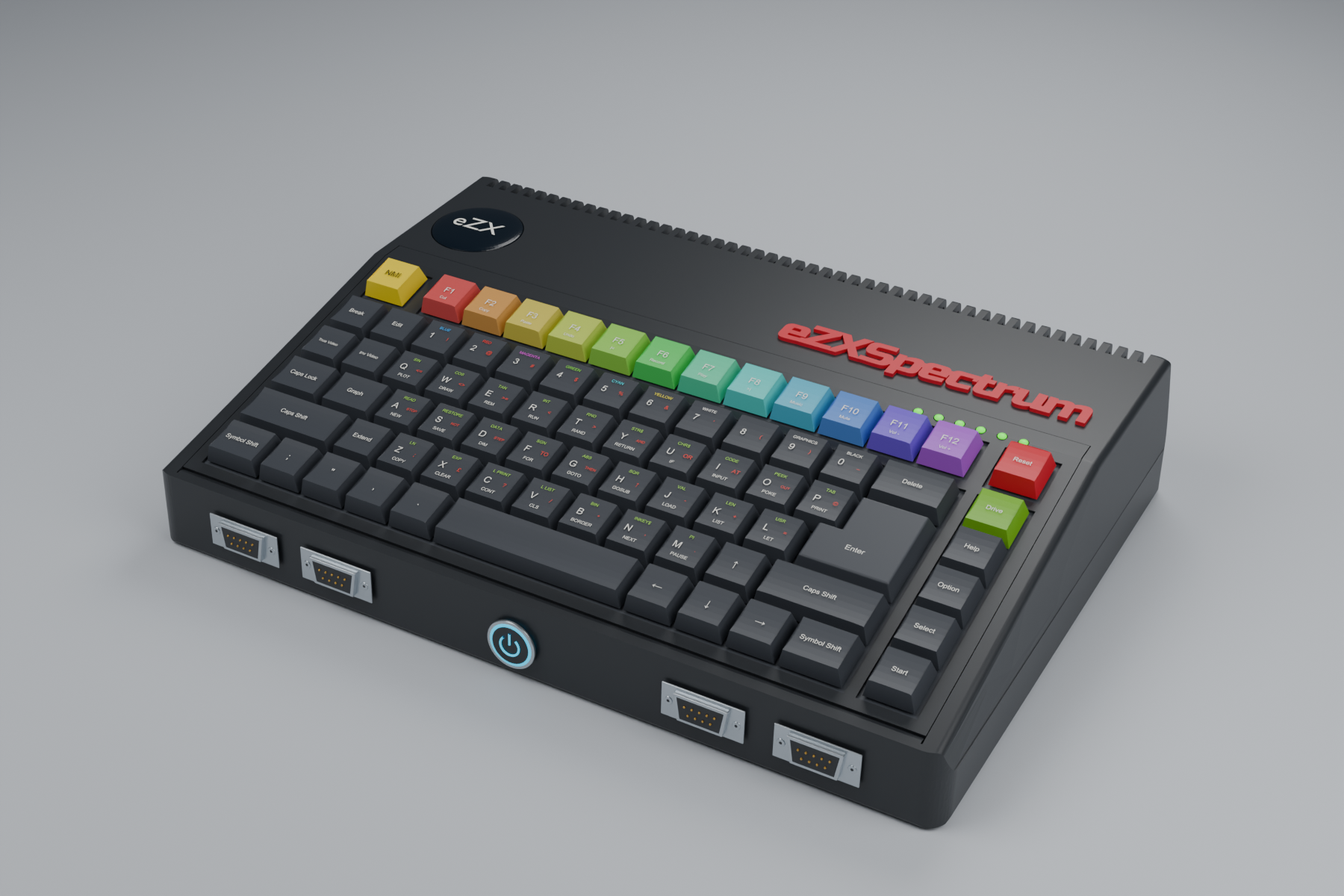
Concept render — black eZX Spectrum enclosure.
Debug support
The Z80 has historically had no hardware debug capability. From the original 1976 Zilog silicon through every clone (NEC, SGS-Thomson, U880) and every modern FPGA reimplementation (T80, TV80, KC80, the Spectrum Next's Z80N), Z80 developers have had to choose between:
- In-circuit emulators (ICE) — expensive add-on hardware that replaced the Z80 socket with debug-instrumented logic. Examples: Periscope, Tek 8540, HP 64000. Routinely costing five-figure sums in their day; entirely unavailable to home computer developers
- ROM monitors — debug code resident in the system ROM that catches NMI / RST vectors, displays registers, allows breakpoints by replacing target opcodes with
RST $38calls. Examples: Spectrum's microdrive-loaded monitors, dezogif on the Spectrum Next, the BBC Micro's MOS debugger. Consume parts of the address space; conflict with software that depends on those vectors; require careful interaction with the running system - Simulator-only debugging — emulators like Fuse, ZEsarUX, CSpect provide debug features that don't exist on real hardware. Developers write code in the emulator, hope it works on real hardware. Discrepancies are common
- Printf-style debug —
BORDERinstructions to indicate progress;BEEPfor audible debug;OUTto a peripheral writing to tape or serial
None of these are equivalent to modern hardware debug. The Z80NG provides genuine hardware debug — the same level of capability that a modern ARM Cortex-M developer takes for granted — surfaced over the FPGA's JTAG path through DeMon. This makes the eZX (in any of its three FPGA images) significantly more productive as a Z80 development platform than any historical Z80 system, including the Spectrum Next.
Debug subsystem capabilities
| Capability | Detail |
|---|---|
| Hardware breakpoints | N programmable address breakpoints (default N = 4 in v1; expandable per LUT4 budget). Each breakpoint specifies a PC address and optional bank-page scope. On match, the CPU halts before executing the instruction at that address |
| Watchpoints | N programmable address-range watchpoints (default N = 4). Each specifies a base address, length, and access type (read / write / read-or-write). On a matching memory access, the CPU halts after the access |
| Single-step | Once halted, the CPU advances exactly one instruction on a debug-port command. Variable-length Z80 instructions are stepped as single units regardless of their byte count |
| Register inspection | All architectural state readable / writable while halted: A, F, BC, DE, HL (and shadows AF', BC', DE', HL'), IX, IY, SP, PC, I, R, IFF1, IFF2, IM |
| Memory inspection | Any address in the running paging context readable / writable while halted, including Z80N's extended paging registers |
| Branch trace ring | Every taken control-flow change (call, ret, jr-taken, jp-taken, conditional-taken, interrupt entry) recorded with PC, target, and timestamp into the host image's HyperRAM. Configurable depth (default: last 1024 branches). On halt, the host debugger reads back the trace for post-mortem analysis |
| Performance counters | Cycles elapsed, instructions retired, branches taken, branches mispredicted, μop cache hits / misses, prefetch buffer fills, memory rendezvous stalls, Z80-equivalent T-states consumed (see Z80-equivalent T-state counter) — all software-readable counters that survive across halts |
Debug halt mechanics
When a breakpoint or watchpoint triggers, the Z80NG pipeline drains cleanly to a defined architectural state, then asserts a debug_halted flag visible over JTAG. While halted:
- The Z80 architectural state is fully stable and inspectable
- Memory reads and writes can be issued by the debugger without disturbing CPU state
- Other chipset elements (display, audio, sprite engine) continue to run — only the CPU is paused
- Interrupts are deferred; they remain pending and fire when execution resumes
- Halt is transparent to software in the sense that no Z80 ISA state changes; the only observable difference is that the CPU isn't progressing
This is significantly cleaner than ROM-monitor debug, which requires the running system to cooperate with the debugger (saving registers via stack pushes, sharing the address space, restoring state on resume). The Z80NG's JTAG-side debug is out-of-band — the running program doesn't know debug exists and can't interfere with it.
Debug across the three images
The same Z80NG debug subsystem serves all three Z80NG-bearing image configurations:
- Next-compatible image — full debug on the 28 MHz Z80N. Better debug story than a real Spectrum Next, which depends on the NMI-driven dezogif workaround. Z80NG turbo mode debug works identically, just at higher CPU clock
- Classic Spectrum image — full debug on the 3.5 / 7 MHz cycle-accurate Z80 per model. Makes the eZX the most debugger-friendly classic-Spectrum platform that has ever existed — original hardware required external ICE pods or ROM monitors with their own compatibility costs
- Third-party FPGA Spectrum projects using Z80NG — inherit the same debug capability if they wire up the JTAG path. The debug subsystem is part of the open-source Z80NG release; no per-licensee work needed
Host protocol
The JTAG-side host protocol is intended to integrate with existing Z80 toolchains (sjasmplus debug output, DeZog, DZRP-compatible debuggers, etc.). The protocol detail is documented separately with the DeMon protocol stack; the Z80NG side simply exposes a debug register block over the JTAG TAP, with the host responsible for protocol decoding. A reference debugger (likely a DeZog extension) will ship alongside the Z80NG release.
This makes the eZX a more capable development target for Z80 / Z80N software than any prior Z80-based system — including the Spectrum Next itself, where developers have long relied on the dezogif workaround. Some Z80 developers may prefer the eZX as their primary development target purely for the hardware debug capability, even if they're targeting real Spectrum Next deployment.
License and origin
Clean-room reimplementation
The Z80NG is an original, independent implementation of the Z80 / Z80N CPU. The clean-room scope is the CPU specifically: the Z80NG does not use, derive from, incorporate, or reference any RTL, schematic, or other source material from the Z80 / Z80N CPU implementation in the upstream NextNano project, nor from the official Zilog Z80 microcode, nor from any other existing Z80 / Z80N CPU implementation. Compatibility with the Z80N ISA is achieved entirely through independent design: opcode behaviour is implemented from the published Z80 documentation and Z80N opcode specifications, timing is implemented from the published Z80 cycle tables, and undocumented Z80 behaviours are implemented from publicly available reverse-engineering documentation of original Zilog silicon.
The rest of the NextNano Spectrum Next FPGA core — display, audio, sprite engine, layer compositing, paging, peripheral subsystems, copper, DMA, NEXTREG infrastructure, and so on — is not subject to this clean-room scope, and the eZX Next-compatible image uses it as-is under its existing licence. The Z80NG drops into that core as a replacement for the upstream Z80N CPU only; everything else around the CPU stays unchanged. This is the same architectural pattern as a CPU swap on real hardware: same motherboard, same peripherals, same display chips — only the processor is different.
This places the Z80NG in the established lineage of clean-room Z80 reimplementations (T80, TV80, KC80, and similar) and follows the standard clean-room methodology used historically for IBM PC BIOS reimplementation, AMD's x86 implementations, and similar IP-respecting compatibility engineering. The Z80NG's open-source release thus gives any FPGA Spectrum-lineage project a CPU it can use without provenance concerns, while the project remains free to use the Next's wider FPGA core under that core's own terms.
Copyright and licensing
The Z80NG RTL source is copyrighted by Anthony Ball / Deluxe Pixel Limited and released under an open-source license (specific license TBD — likely MIT, Apache 2.0, or BSD-class permissive to maximise reuse by other FPGA Spectrum-lineage projects).
Permissive licensing reflects the architectural goal: the Z80NG should become the canonical clean-room Z80N implementation that any FPGA Spectrum project can adopt, freeing the broader community from any concerns about Z80N source provenance. The Z80NG provides:
- A documented, independent Z80N ISA implementation
- Modern microarchitectural features (prefetch buffer, μop cache, turbo mode) usable by any host
- A clean copyright story for projects that need it (commercial Spectrum-lineage hardware, educational use, derivative compatibles)
Reuse and attribution
Projects incorporating the Z80NG must retain the copyright notice and license text. Modifications are permitted; redistribution of modified versions must be clearly identified as such (not as the canonical Z80NG). The Z80NG name itself is reserved for the upstream design — derivatives should use a different name to avoid confusion.
What this is not
- The Z80NG is not a Zilog Z80 in silicon — it's an FPGA soft core
- The Z80NG is not a derivative of the NextNano Z80 / Z80N CPU implementation — it's an independently designed CPU that drops into the rest of the Next core in place of it
- The Z80NG is not binary-compatible with anything other than the Z80 / Z80N ISA — it does not implement eZ80 (Zilog's 16-bit Z80 successor) instructions, Rabbit Semiconductor extensions, or other Z80-derivative ISAs
- The Z80NG is not a microcode emulator — it's a hardware pipeline that directly executes the Z80N ISA
Future directions
Beyond v1, possible additions include:
- Z80NG-extended ISA (planned for v2) — the FPGA-native instructions described under Beyond cycle compression. Wide arithmetic, parallel byte ops, hardware-paced block ops, bit-field operations, etc. Optional and detected via feature register; never on by default in Z80 / Z80N modes
- Dual-issue execution — for very tight loops in turbo mode, executing two non-conflicting Z80 instructions per cycle. The BSRAM-fmax ceiling still applies, but each cycle delivers more work
- Larger μop cache configurations — 32 KB or 64 KB for projects with BSRAM headroom (depends on host image's BSRAM allocation)
- Branch-pattern prefetcher — anticipatory μop pre-translation based on observed branch behaviour, eliminating cold-miss decode latency for repeatedly-visited code regions
- Hardware DSP integration — exposing the FPGA's DSP blocks as Z80NG-accessible function units for game-engine-relevant math (matrix transforms, fixed-point trig, etc.)
These are out of scope for the initial Z80NG v1 design. The first release targets Z80N binary compatibility, cycle-accurate per-model timing for the Classic image, and the turbo mode cycle-compression showcase. The μop cache and windowed prefetch buffer are the headline v1 microarchitectural features.